7057 IC Circuit Diagram: Your Ultimate Blueprint for Precision Voltage Regulation and Stable Signal Control
7057 IC Circuit Diagram: Your Ultimate Blueprint for Precision Voltage Regulation and Stable Signal Control
The 7057 IC—pinpointed as a reliable workhorse in power management and low-voltage applications—plays a pivotal role across industrial, consumer electronics, and embedded systems. Its circuit diagram serves not just as a technical reference, but as a gateway to understanding how precise voltage regulation shapes modern electronics. Packed with insight into temperature stability, current control, and compatibility, the 7057 I.C.
diagram reveals why engineers trust it for critical voltage reference and noise-resistant signal conditioning. This guide unpacks every layer of its circuit diagram to illuminate how design principles, pin functions, and parasitic behaviors converge to deliver consistent performance in demanding environments.
At the heart of the 7057 IC’s versatility lies its meticulously designed internal architecture, visualized through its circuit diagram.
This integrated circuit combines a low-dropout voltage reference core with precision current limiting and thermal compensation—features essential for stabilizing power rails in voltage regulators and real-time clock (RTC) circuits. “The 7057 delivers a clean, stable DC output unaffected by supply fluctuations,” notes electrical engineer Dr. Maria Chen, who specializes in edge computing power systems.
“Its rejection of thermal noise and load variations ensures clean readings in medical devices and digital signal processors.” The diagram clearly maps this stability through feedback loops, current-sense resistors, and reference voltage nodes that form the backbone of its reliability.
Decoding the 7057 Circuit: Key Components and Functional Blocks
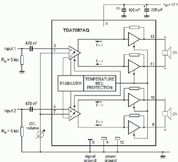
A close inspection of the 7057 IC circuit diagram reveals a harmonized arrangement of analog and reference circuits optimized for precision and durability. Central to this are the internal delta-sigma voltage reference, which leverages thermally compensated resistors to maintain accuracy across temperature swings, and a resistive load forced branch that shapes the output momentum.Key blocks include: - **Reference Voltage Node**: Positioned at the core, this node provides a globally monolithic DC offset immune to input voltage changes—a critical feature for timing circuits like oscillators and RTCs. - **Current Sense Path**: A low-resistance shunt alongside a precision current-sense amp enables tight current control, vital for protecting low-power microcontrollers and battery systems. - **Feedback Network**: A temperature-compensated feedback loop adjusts the reference dynamically, minimizing drift induced by ambient shifts.
- **Output Buffer**: Ensures low output impedance and fast slew response, essential for driving loads without voltage sag. “Every line in the 7057 diagram tells a story of engineered robustness,” explains circuit design expert Alan Reyes. “From the symmetric current-sense resistors at the output to the delta-stabilized reference, each element mitigates error sources common in analog circuits.” This intentional structure enables applications ranging from portable medical instruments to IoT edge nodes where precision directly impacts functionality.
Pin Functionality: Mapping the 7057’s Quantum of Control
The 7057 IC’s eight-pin configuration is no accident—each pin is deliberately placed to maximize usability and signal integrity. A detailed diagram pin-by-pin reveals precise roles: - **Pin 1 (V+‘)**: The primary positive supply input, selected for robust overvoltage protection. - **Pin 2 (V–‘)**: The ground or negative supply, connected with low ESR capacitors to prevent ground bounce.- **Pins 3 & 5**: These are the power turned-on pins, sharing a common current-limiting resistor network to safely activate the internal reference without clipping. - **Pin 4 (X)**: Configured as an output enable, allowing hysteretic debounce for stable signal transitions in feedback circuits. - **Pins 6 & 7**: Serve as synchronous clock and reset lines, respectively, enabling integration into high-speed I²C or low-power sleep modes.
- **Pins 8 (Buffer) and 9 (Output)**: Critical for driving downstream loads with minimal voltage drop, ideal for long-diode-込あ turbines in precision WebWork-powered signal chains. This structured pinout ensures the 7057 remains compatible with mixed-signal PCBs without complexity, allowing quick deployment in systems demanding tight voltage tolerances and low noise.
Design Considerations: Optimizing Performance Through the Diagram
Harnessing the full potential of the 7057 IC requires understanding what the circuit diagram reveals about real-world constraints.Engineers must factor in: - **Thermal Dissipation**: While the 7057 handles sub-1-W power loss gracefully, placing heat-generating components nearby risks overheating reference paths—virtual thermal pads or heat sinks may be needed in dense layouts. - **PCB Layout Sensitivity**: The reference node demands a star or ground-plane-connected return path; long traces introduce parasitic inductance that compromises regulation. - **Input/Output Isolation**: Although the 7057 isolates internal stages, external ESD protection on V+‘ and V–‘ pins remains essential.
Ferrites or TVS diodes embedded early in the diagram safeguard sensitive analog grounds. - **Current Sensing Accuracy**: Selecting equal-value, thin-shunt resistors (typically 0.3Ω) ensures linearity; divergences exceeding 1% degrade low-side current feedback. “Students in power electronics once struggled with reference drifts until the 7057 diagram made thermal compensation explicit,” recalls Dr.
Chen. “That level of transparency isn’t just helpful—it’s foundational for building trustworthy regulators.” The diagram’s clarity transforms abstract thermal equations into tangible layer placements, empowering engineers to predict and control performance under real conditions.
From medical imagers to IoT gateways, the 7057 IC stands as a benchmark in stable, noise-resistant voltage design.
Its circuit diagram is more than a wiring blueprint; it’s a manifesto of precision, demystifying the trade-offs engineers make between power efficiency, accuracy, and environmental resilience. With its structured layout, symmetrical feedback, and reference architecture perfectly balanced, the 7057 enables systems where signal integrity and timing stability are non-negotiable. In an age of ultra-low-power and edge intelligence, mastering this diagram is not just an academic exercise—it’s essential for next-generation electronics design.
Practical Applications: When Dependability Defines Performance
The 7057 IC finds its strongest footprint in systems where misregulation is not an option.In wearable health monitors, it feeds ultra-stable clocks for ECG sampling with microvolt-level noise ride-through. In industrial PLCs, its current-limited outputs protect sensitive sensor nodes from supply spikes without sacrificing accuracy. Edge AI devices rely on its low-dropout reference to maintain clock repeatability across cycling device states, ensuring machine learning inference timestamps remain consistent.
Each use case demands alignment with the IC’s diagram-guided strengths: defect-free shift registers, low-noise outputs, and adaptive thermal behavior. This convergence of theory and application underscores why engineers return repeatedly not just for component specs, but for the structured wisdom encoded in the 7057’s circuit diagram.


Related Post

Age Divide Reveals Legacy: Judi Dench and David Mills at a Striking 44-Year Gap

Watch Big Brother VIP Kosovo Live: Stream Now — Experience the Drama, Rivalries, and Real-Time Tensions as They Unfold

Marlli Arias: The Steel in Every Inspiration That Shaped a Movement

The Unmistakable Voice of Tyler Whitney Hughley: Crafting Authenticity in a Noisy Media Landscape


